DAC and PWM KiCad Simulation
In this post we are going to create a PWM source that is fed into an RC low pass filter to convert the PWM signal into a rough analog signal. Next, we will pass the output of the RC low pass filter into an RC high pass filter that will remove the DC offset and give us the ability to control the peak to peak voltage value of the output. We are writing this as a supplemental post relating to our series on the Puppy Patrol MK1 and will simulate a 250Hz and 500Hz output as they are related to that series.
TL;DR
Here are the files for the project
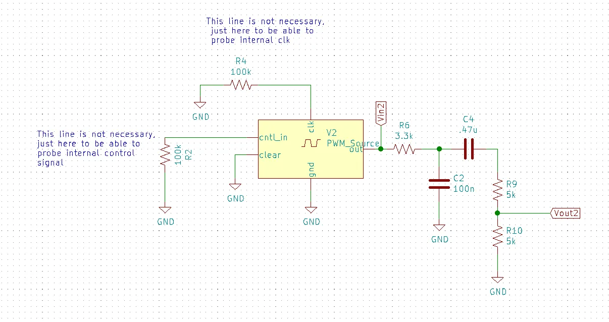
Here is the final subcircute we will be creating
.subckt pwm_source  clk cntl_in clear out gnd
*****************************************************************
* freq = frequency of control signal
* sample_rate = number of pwm pulses per control signal cycle
*****************************************************************
.param freq=250 sample_rate=10
ain clk cntl_in clear out pulse2
*****************************************************************
* create output by sampeling the control signal every negative
* edge of the clk and firing a square with a lingth determined by the
* line (-5.1, 0), (5.1, 1/(freq*sample_rate)) => -5v = no pulse 0v = 1/2 clk cycle
* 5v= 1 clk cycle.
* used -5.1 and 5.1 because -5.0 and 5.0 would cause the pulse to not work at the
* peak and min voltage
*****************************************************************
.model pulse2 oneshot(cntl_array = [-5.1 5.1]
+                     pw_array=[0 {1/(freq*sample_rate)}]
+                     clk_trig = 0.9 pos_edge_trig = FALSE
+                     out_low = 0.0 out_high = 5
+                     rise_delay = 20.0e-9 fall_delay = 35.0e-9)
*****************************************************************
* create clock signal
*****************************************************************
Vclk clk gnd dc 0 pulse(0 1 2n 2n 2n {1/(freq*sample_rate*2)} {1/(freq*sample_rate)})
*****************************************************************
* create control signal
*****************************************************************
Vsignal cntl_in gnd dc 0 sin(0 5 freq)
.ends
PWM – Pulse Width Modulation
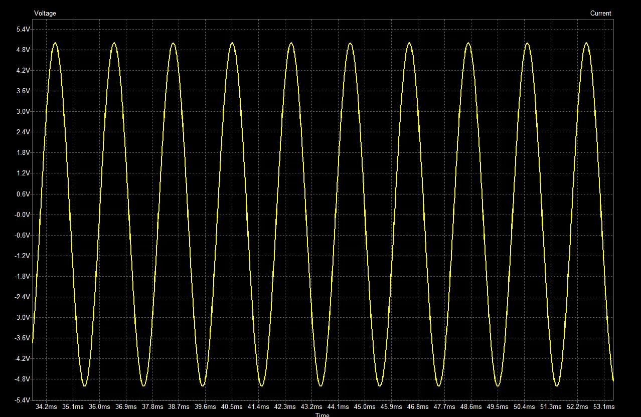
Pulse width modulation is the processing of changing a digital pulses width proportional to some input. One reason you may want to do this is many microcontrollers only have digital outputs. That means if you need to generate an audio signal with only digital outputs than you will need something like PWM to encode the signal. To demonstrate how to use PWM to encode an audio signal will first take a sample signal of 500Hz and simulate it in KiCad via this ngspice command
Vsignal cntl_in gnd dc 0 sin(0 5 500)
- Vsignal = Voltage component with the name Vsignal (see 2.1.3 for more info)
- cntl_in = first connected net
- gnd = second connected net
- dc 0 = dc offset of 0
- sin = generates the sin wave and is described in section 4.1.2 of the ngspice manual
Then create a clock that will sample the 500 Hz tone 5 times per cycle
Vclk clk gnd dc 0 pulse(0 1 2n 2n 2n {1/(500*5*2)} {1/(500*5)})
- Vclk = Voltage compoenet named Vclk (see 2.1.3 for more info)
- clk = fist net connection
- gnd = second net connection
- dc 0 = dc offset of 0
- pulse = generates the square wave and is described in section 4.1.1 of the ngspice manual
- 500 = Frequency
- 5 = sample rate
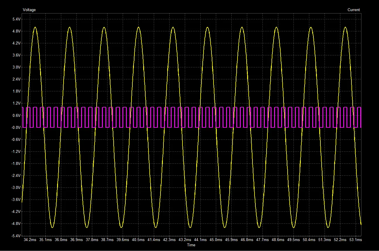
Next we will create a square wave that samples the 500Hz signal on the negative edge of the clock and outputs a pulse width is proportional to the voltage value of the sample tone.
ain clk cntl_in clear out pulse2
.model pulse2 oneshot(cntl_array = [-5.1 5.1]
+                     pw_array=[0 {1/(freq*sample_rate)}]
+                     clk_trig = 0.9 pos_edge_trig = FALSE
+                     out_low = 0.0 out_high = 5
+                     rise_delay = 20.0e-9 fall_delay = 35.0e-9)
- ain = XSPICE component named ain (see 2.1.3 for more info)
- clk = first connected net
- cntl_in = second connected net
- clear = third connected net
- out = fourth connected net
- pulse2 = model to use
- .model pulse2 oneshot = defines a model named pulse2 that uses the oneshot XSPICE function. More on oneshot can be found in section 12.2.24 Controlled One-Shot
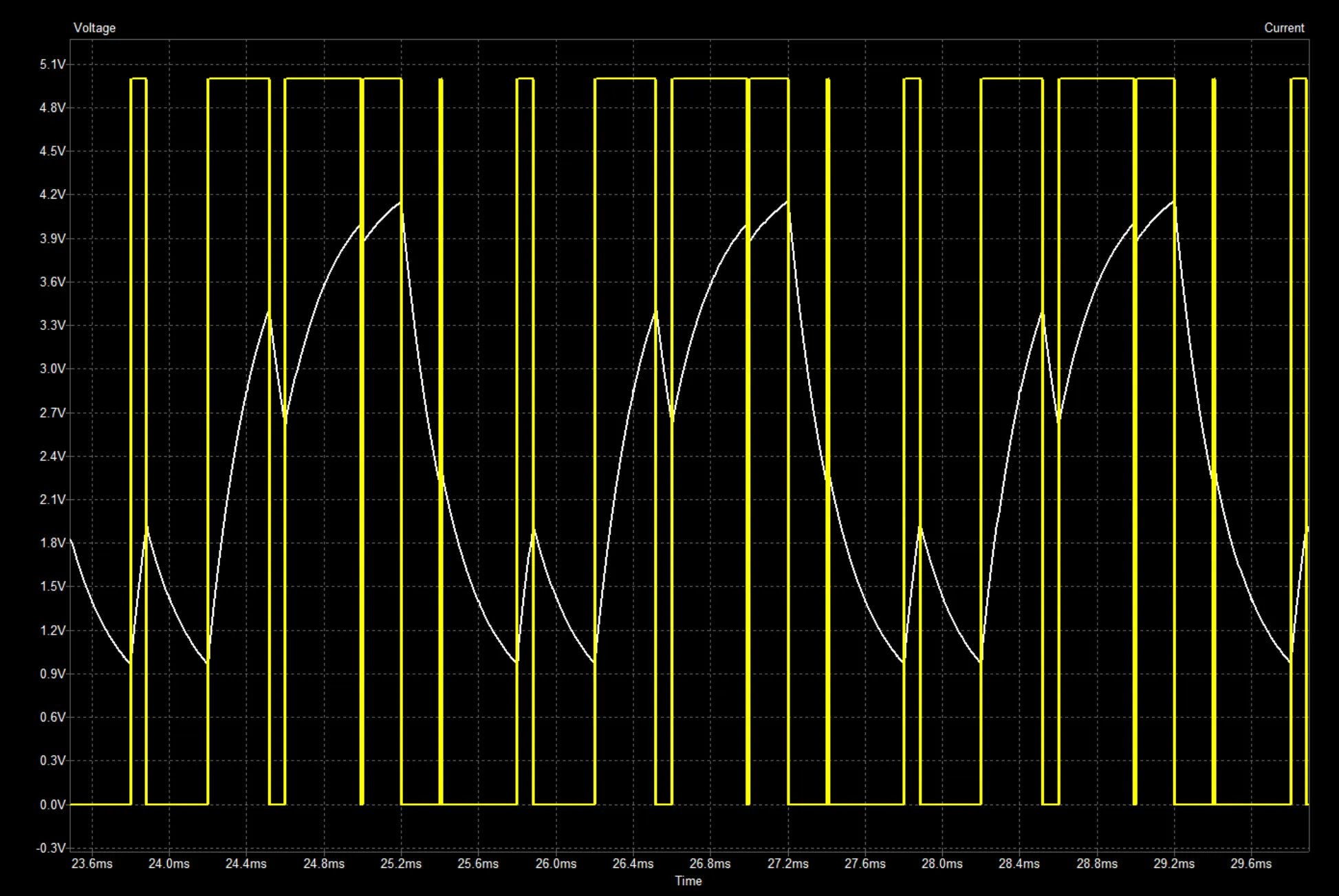
From the image above you can see how the blue pulses are representing the yellow analog signal by changing their pulse width proportional to the yellow signal’s voltage value. This is a way that PWM can be used to digital represent an analog signal.
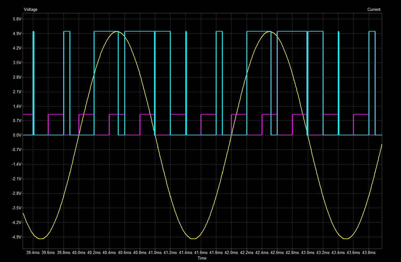
Next, the PWM signal is connected to a low pass filter that will produce convert the digital PWM signal into a jagged sin wave of the original 500 Hz signal.
This signal is created by the capacitor in the low pass filter charging and discharging as the PWM signal goes high than low. It is easier to see with the PWM signal overlayed on top of the low pass filter’s output.
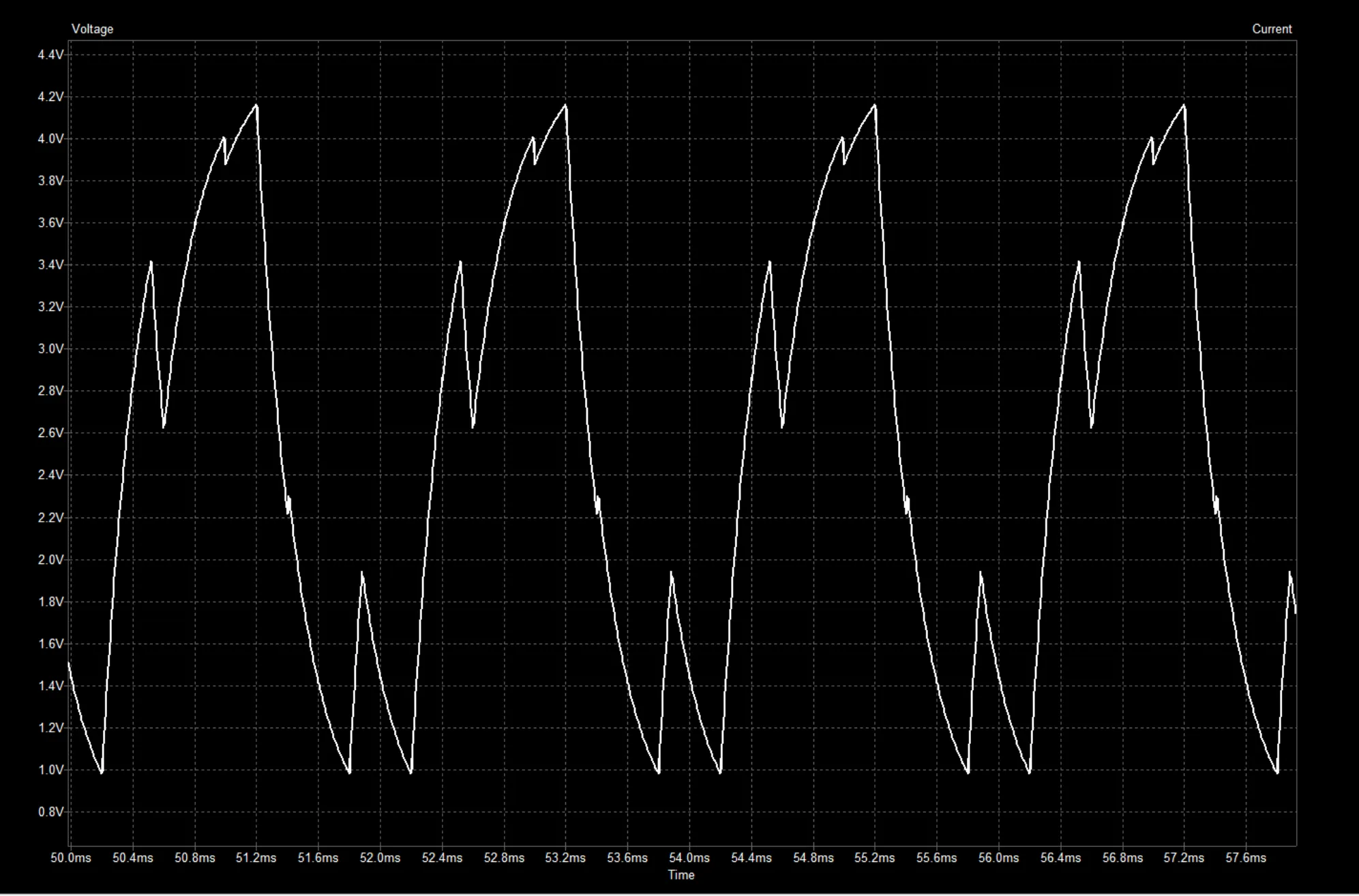
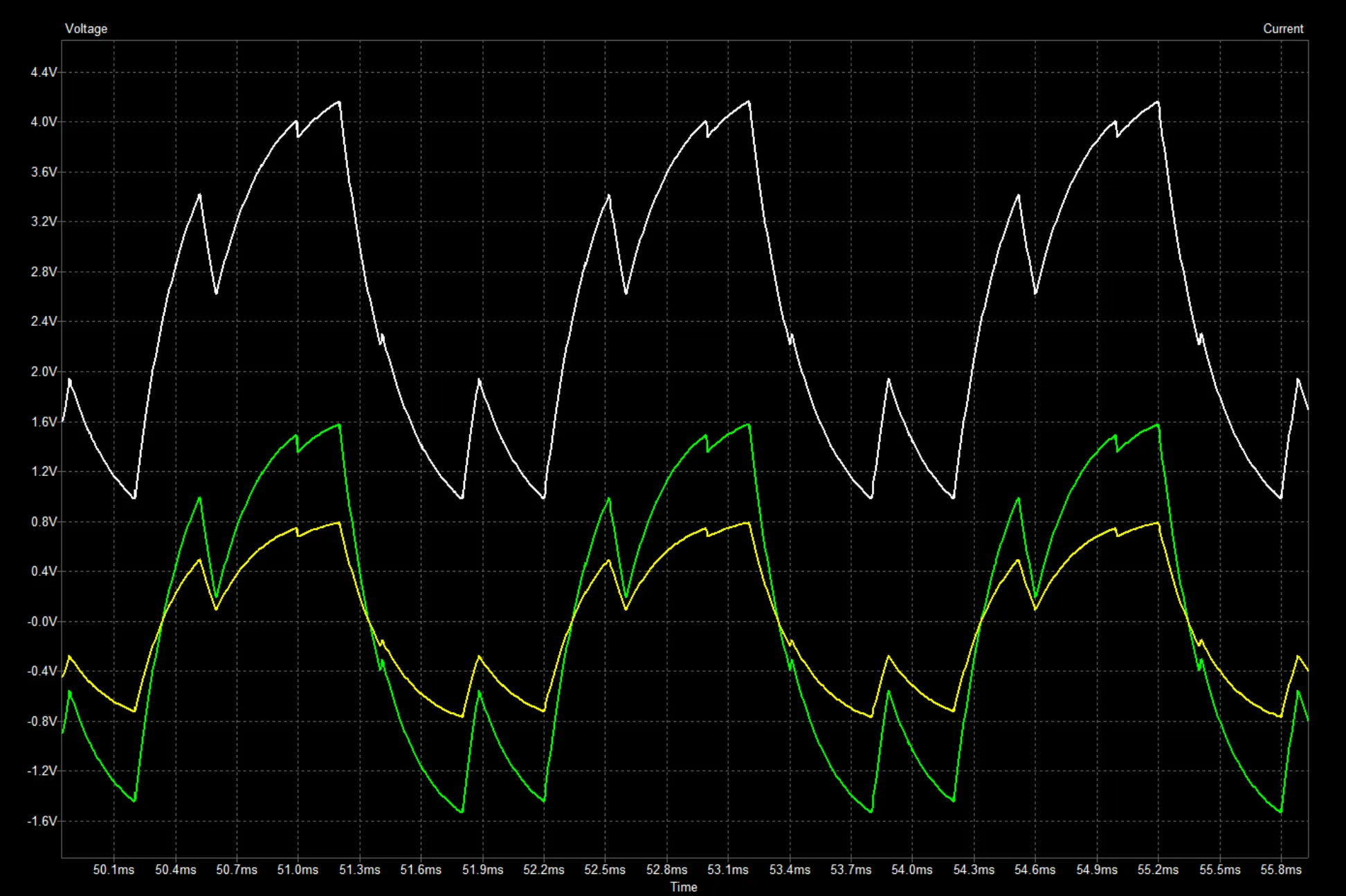
The next stage of the circuit is built to remove the DC offset by using a decoupling capacitor (green signal) and then run the signal through a potentiomotrer that will be used to control the volume (yellow signal).
Below is the circuit that we created and here is a link to a video showing what we just discussed.
Here is a video of us creating this circuit
Here is the subcircuit
ain clk cntl_in clear out pulse2
*****************************************************************
* create output by sampeling the control signal every negative
* edge of the clk and firing a square with a lingth determined by the
* line (-5.1, 0), (5.1, 1/(freq*sample_rate)) => -5v = no pulse 0v = 1/2 clk cycle
* 5v= 1 clk cycle.
* used -5.1 and 5.1 because -5.0 and 5.0 would cause the pulse to not work at the
* peak and min voltage
*****************************************************************
.model pulse2 oneshot(cntl_array = [-5.1 5.1]
+                     pw_array=[0 {1/(500*5)}]
+                     clk_trig = 0.9 pos_edge_trig = FALSE
+                     out_low = 0.0 out_high = 5
+                     rise_delay = 20.0e-9 fall_delay = 35.0e-9)
*****************************************************************
* create clock signal
*****************************************************************
Vclk clk gnd dc 0 pulse(0 1 2n 2n 2n {1/(500*5*2)} {1/(500*5)})
*****************************************************************
* create control signal
*****************************************************************
Vsignal cntl_in gnd dc 0 sin(0 5 500)
.ends
Expanding on the subcircuit
The example we went over is great for a 500 Hz signal but if we want to reuse the block to produce botha 500 Hz and 250 Hz ouput we can slightly modify the setup to allow for parameters to be passed in.
First we add the parameters to our subcircuit, the 250 and 10 are default values
.param freq=250 sample_rate=10
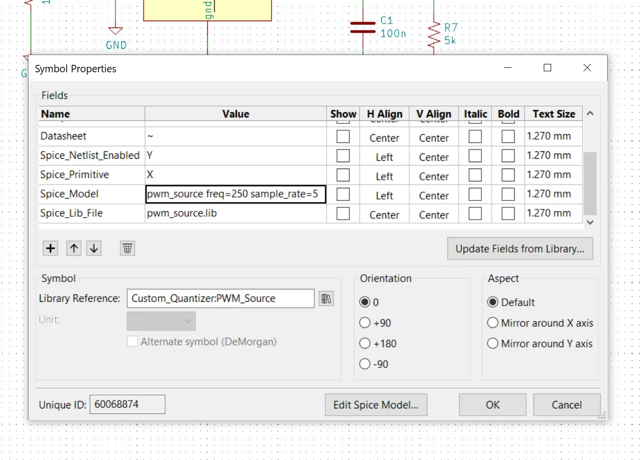
Next we pass in the two parameters when setting the spice model in KiCad
pwm_source freq=250 sample_rate=5
Lastly we update our subcircut to use the parameters. Here is the completed subcircuit
*****************************************************************
* freq = frequency of control signal
* sample_rate = number of pwm pulses per control signal cycle
*****************************************************************
.param freq=250 sample_rate=10
ain clk cntl_in clear out pulse2
*****************************************************************
* create output by sampeling the control signal every negative
* edge of the clk and firing a square with a lingth determined by the
* line (-5.1, 0), (5.1, 1/(freq*sample_rate)) => -5v = no pulse 0v = 1/2 clk cycle
* 5v= 1 clk cycle.
* used -5.1 and 5.1 because -5.0 and 5.0 would cause the pulse to not work at the
* peak and min voltage
*****************************************************************
.model pulse2 oneshot(cntl_array = [-5.1 5.1]
+                     pw_array=[0 {1/(freq*sample_rate)}]
+                     clk_trig = 0.9 pos_edge_trig = FALSE
+                     out_low = 0.0 out_high = 5
+                     rise_delay = 20.0e-9 fall_delay = 35.0e-9)
*****************************************************************
* create clock signal
*****************************************************************
Vclk clk gnd dc 0 pulse(0 1 2n 2n 2n {1/(freq*sample_rate*2)} {1/(freq*sample_rate)})
*****************************************************************
* create control signal
*****************************************************************
Vsignal cntl_in gnd dc 0 sin(0 5 freq)
.ends